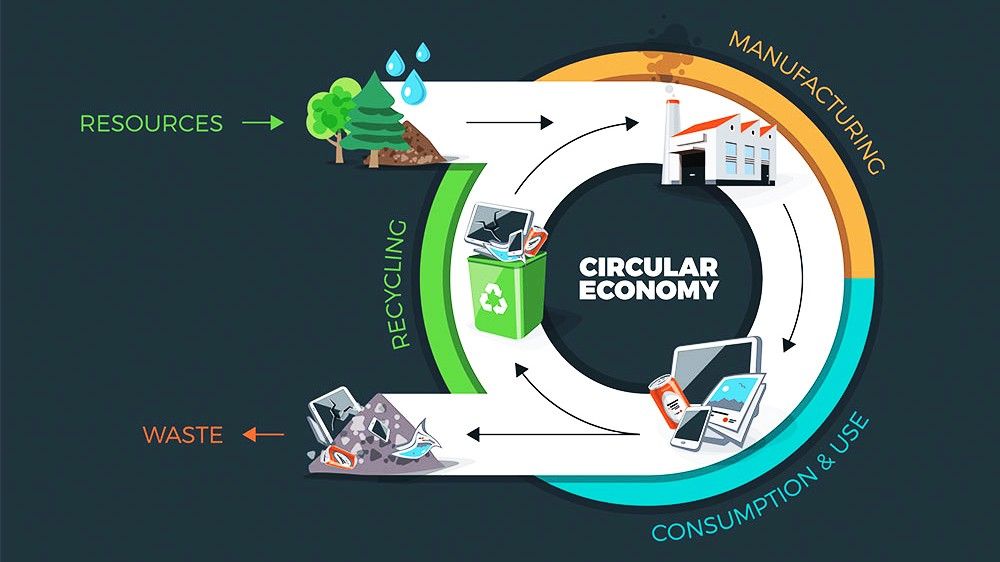
The semiconductor industry is adopting a circular economy approach to minimize waste and maximize resource efficiency. With fabrication processes consuming vast amounts of materials, water and energy, manufacturers are now focusing on recycling, material recovery and closed-loop systems to create a more sustainable production cycle. Erik Hosler, a specialist in semiconductor innovation and materials science, highlights the role of material development in shaping a more sustainable future for semiconductor manufacturing.
Recycling Rare and Critical Materials
The semiconductor industry relies on rare and valuable materials, such as gallium, indium, platinum-group metals and rare earth elements. These elements are critical for chip fabrication but are often sourced through environmentally disruptive mining processes.
To address this, fabs are integrating advanced material recovery systems that extract and reuse valuable metals from production waste. Instead of discarding used materials, manufacturers are now refining and reintegrating them into the fabrication cycle. This reduces reliance on new raw materials, lowers costs and decreases the overall environmental footprint of semiconductor production.
“Material development is essential for improvements in power and performance of transistors at each technology node and now it is the key for enabling long-term sustainability,” says Erik Hosler. By advancing material science, fabs can ensure that semiconductor production becomes more resource-efficient while maintaining high performance and reliability.
Water Recycling and Ultra-Pure Water Systems
Semiconductor fabrication is water-intensive, requiring Ultra-Pure Water (UPW) to clean wafers and prevent contamination. Traditionally, large volumes of water are used once and then discarded, contributing to significant waste.
To close the loop, manufacturers are adopting closed-loop water recycling systems that filter and reuse ultra-pure water multiple times before disposal. These systems help fabs reduce freshwater consumption, lower wastewater discharge and improve overall water efficiency. Some semiconductor facilities have implemented advanced filtration and desalination technologies that allow up to 75% of water to be reclaimed and reused within the manufacturing process.
Reducing Waste Through Process Optimization
In addition to material and water recycling, semiconductor fabs are focusing on process optimization to minimize overall waste. Advanced lithography techniques, such as Extreme Ultraviolet (EUV) lithography, reduce the number of process steps required for chip fabrication. Fewer steps mean less chemical usage, lower energy consumption and reduced waste generation.
A More Sustainable Future for Semiconductor Manufacturing
As semiconductor companies embrace circular economy strategies, they are proving that technological progress and environmental responsibility can go hand in hand. By investing in recycling systems, material recovery and water reuse, fabs are reducing waste, conserving resources and lowering emissions. This shift toward circularity ensures that the semiconductor industry remains innovative, resilient and environmentally conscious in the years to come.

